The bipolar junction transistor is derived from three words, bi, junction, and transistor. The junction refers to the p-n junction that allows the flow of charge carriers and the current in a particular direction. The transistor is a three terminal semiconductor device that regulates the flow of current. The word 'bi' means two. Thus, BJT is a device that has three terminals (emitter, base, and collector), two p-n junctions, with the three separately doped regions.
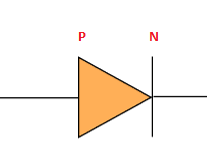
The p-n junction is made of two doped regions 'p' and 'n.'
The p region has majority charge carriers holes (possesses positive charge), and the n region has majority charge carriers electrons (possesses negative charge). The charge moves from the high concentration (emitter) region towards the low concentration (collector). The emitter junction in BJT is highly doped.
BJT is also known as the current controlled device. It is because the input current determines its output.
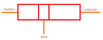
The three terminals of the Bipolar Junction Transistor are shown below:
A single p-n junction transistor is shown below:
Here, we will discuss the following topics:
Modes of operation of BJT
Breakdown voltages of BJT
Transistor Switching in BJT
Let's start.
What is BJT?
Let's first discuss the three configuration of the BJT before proceeding with its working.
The three terminals of BJT are as follows:
1. Emitter
The emitter region is the highly doped region as compared to the other two regions of the transistor. It is the region where the charge starts flowing. It means that the charge flows from the emitter to the collector.
2. Base
The base region is the smallest region of the transistor. It is small to avoid carrier recombination. It will stop the electrons and holes from recombining and will pass more electrons towards the base region. It has the opposite polarity from the emitter and the collector region.
3. Collector
The collector region is the lightest doped region. It is often connected in reverse biased with the base, which does allow any charge flow. It receives charge carriers from the base. In amplifiers, it is considered as the output region. The collector region has the maximum width among the three region of the BJT.
Voltage Bias
There are two types of voltage bias, i.e., forward bias and reverse bias.
Forward bias
The forward bias is the connection of the transistor, where the (+) terminal of the battery is connected with the region containing positive charge carriers (p region) and (-) terminal with the region containing negative charge carriers (n region).
Reverse bias
The battery's positive terminal is connected with the region containing negative charge carriers (n region) and the negative terminal containing positive charge carriers (p region). We can say that the connection is opposite as compared to the forward bias. The flow of charge in case of reverse bias is zero. It is because the contact of the junction has two charges of opposite nature, which attracts them. It pulls the charge from the junction making the depletion region or base wider, which does not allow the charge to flow easily.
In the case of BJT, the base-emitter region is connected in the forward bias, and the base-collector region is connected in the reverse bias.
Types of BJT
There are two types of Bipolar Junction Transistor, NPN transistor and PNP transistor.
NPN Transistor
The NPN transistor consists of one P-doped region between the two N-doped regions.
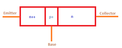
The structure of the NPN transistor is shown below:
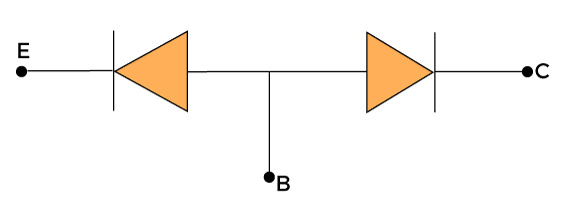
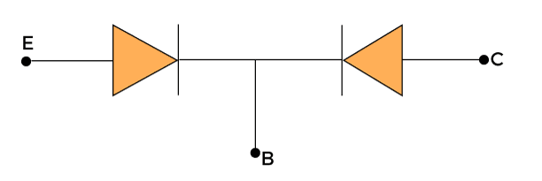
The equivalent circuit of an NPN transistor as a combination of the two p-n junctions is shown below:
The '++' sign indicates the heavy impurity doping concentrations, while the '+' indicates the moderate impurity doping concentration. A p slab is inserted between the two n slabs forming an NPN semiconductor. Here, the emitter junction 'n++' is heavily doped, and the collector junction 'n+' is lightly doped.
Working of NPN transistor
Connection Setup: The battery's negative terminal (VEE) is connected to the emitter n++ slab and the battery's positive terminal (VCC) to the collector n+ slab. The above connection is also known as the forward-active operating mode.
The circuit and symbol of NPN is shown below:
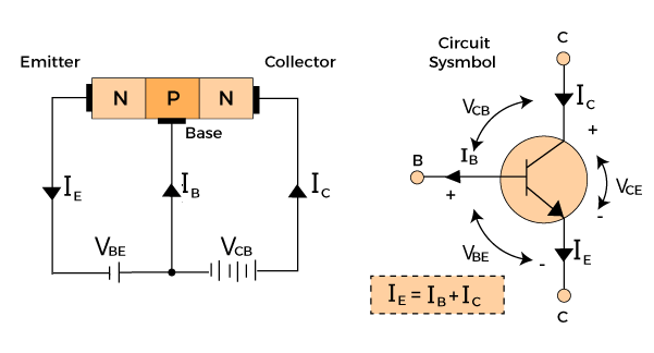
Working: When the battery is switched ON, the electrons from the battery flow to the n++ emitter. Both the battery and n region consists of negative charged electrons. The same charge repels each other, and the electrons starts moving away from the emitter towards the base region. The p+ slab has minority carriers' electrons and majority carriers' holes. The flow of electrons from the emitter increases the minority carrier concentration in the base region and it starts flowing towards the collector region. The flow of charge at the base-collector region is zero because of reverse biased. The flow of current is always opposite to the flow of electrons. Hence, the current flows from the collector to the emitter.
PNP Transistor
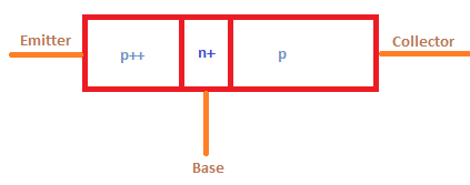
The PNP transistor consists of one N-doped region between the two P-doped regions.
The structure of the PNP transistor is shown below:
The equivalent circuit of a PNP transistor as a combination of the two p-n junctions is shown below:
Here, an n slab is inserted between the two p slabs made of semiconductor material. The emitter junction 'p++' is heavily doped and the collector junction 'p+' is lightly doped.
Working of PNP transistor
Connection Setup: The battery's positive terminal (VEE) is connected to the emitter p++ slab and the battery's negative terminal (VCC) to the collector p+ slab.
The circuit and symbol of the PNP transistor are shown below:
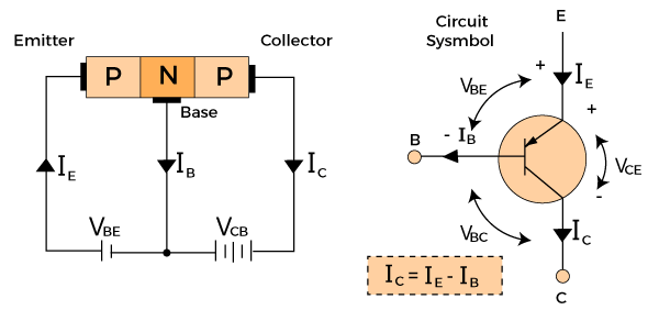
Working: The electrons flow from the negative terminal of the battery to the positive terminal. When the battery is switched ON, the positive charge flow to the p++ emitter region, which consists of the majority, charged holes. The same charge repels each other, and the holes start moving away from the emitter towards the base region. The n+ slab has majority carriers' electrons and minority carriers' holes. Due to the small width of the base, a few holes combine, and the rest move towards the collector. It constitutes a very small current in the base region. The flow of charge at the base-collector region is zero because of reverse biased. The direction of the current is the same as the direction of the flow of holes.
Hence, the current flows from the emitter to the collector. The current direction is in the opposite direction compared to the NPN transistor because of the majority carriers.
Note: The formation of current in the NPN transistor is due to the majority carriers' electrons. The formation of current in the PNP transistor is due to the majority carriers' holes.
Regions of operation
There are three regions of operation in Bipolar Junction Transistors, which are listed as follows:
- Forward active region
- Cut-off region
- Saturation region
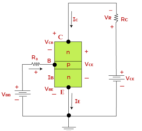
Let's discuss the above four regions of BJT. Here, we will consider the NPN transistor for further explanation. The NPN bipolar junction transistor configuration with the emitter junction as the input is shown below:
Forward active region
It is the region of operation when the base-emitter junction is forward-biased. The flow of electrons from the emitter to the base and to the collector results in the emitter current and the collector current. The KVL equation for the collector-emitter loop can be written as:
VCC = ICRC + VCB + VBE = VR + VCE
Where,
VCC: It is the voltage across the C
IC: It is the collector current
RC: It is the resistance across the C
VCB: It is the voltage across the C - B junction
VBE: It is the voltage between the B and the E region. For the silicon transistors, the VBE is 0.7 Volts.
VR: It is the threshold voltage
VCE: It is the voltage across the C - E junction
The C - E loop is shown in the above image.
Cut-off region
Cut-off region refers to the state of the transistor when all the currents flowing in the circuit are zero. It occurs when the voltage across the B - E junction is considered as zero or reverse biased. The absence of current causes no movement of electrons emitter junction, thus no emitter current. The B - C junction is already reverse biased. Hence, all the currents (base current, collector current, and emitter current) are zero.
Saturation region
The increase in forward bias voltage results in the movement of electrons towards the base region. It further increases the emitter and the collector current. When the collector current increases, the threshold voltage across the resistor also increases.
The state of the current flow in the three regions is shown in the below diagram:
In the saturation mode, both the B - E region and the base- collector region are forward biased. For the large value of C - E voltage, the base region becomes reverse biased and for the small value of C - E voltage, the base region becomes forward biased.
The load line superimposed on the BJT characteristics is shown below:
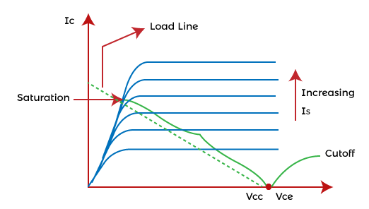
The load line can be used to depict the operating mode of the transistor.
The Kirchhoff voltage equation for the C - E configuration can be written as:
VCE = VCC - ICRC
Transistor currents
There are three transistor currents flowing in the BJT circuits, which are emitter current, base current, and collector current.
Collector current
The base-emitter voltage controls the collector current in the transistor. It is because the collector-base junction is reverse biased and does not possess its current. It is given by:
IC = IS exp (VBE/VT)
We can also say that the collector current is equal to the emitter current generated when the electrons are injected from the emitter to the base.
Emitter current
The emitter current is represented by IE1. It flows due to the movement of electrons from the emitter to the base. The injected holes in the base region also produce the current IE2. It is the part of the Base-emitter junction only and does not contribute to the collector region. We can write the equation as:
IE2 = IS2 exponential (VBE/VT)
Where,
VBE: It is the voltage between the base and the emitter region. For the silicon transistors, the VBE is 0.7 Volts.
VR: It is the threshold voltage
IS2: It is the current due to the minority carrier holes in the emitter region
Total emitter current is:
IE = IE1 + IE2
IE = IC + IE2
Here, IE1 is equal to the collector current, as discussed above.
IE = ISE exp (VBE/VT)
The ratio of the collector current and the emitter current is given by:
IC/IE = a
Where,
a is the common-base current gain and its value is generally less than 1.
Base current
The emitter current is represented by IB. In case of the NPN transistors, the majority carriers in the base are holes. The holes start disappearing due to the injection of large electrons or some recombination of the charge carriers. Hence, the holes are resupplied to the base terminal to balance the positive charged holes, which constitutes the base current. The number of recombination of electrons and holes in the base depends on the presence of minority carrier electrons.
Thus, the base current is proportional to:
IB = exponential (VBE/VT)
IB = exp (VBE/VT)
The ratio of the collector current and the base current is given by:
IC/IB = B
Where,
B is the common-emitter current gain and its value is generally greater than 1.
Advantages of BJT
The advantages of Bipolar Junction Transistors are as follows:
- It can operate in both the low and high power applications and can perform well at high frequencies.
- Large gain bandwidth
It has large gain bandwidth due to the current density and high voltage gain. - High current density
It means that the amount of current per unit time flows through a per unit cross-sectional area. - High voltage gain
It means more current output for the desired input. The voltage gain is the ratio of the output to input. So, if the output is high, the voltage gain of the BJT will also be high.
Disadvantages of BJT
The disadvantages of Bipolar Junction Transistors are as follows:
- Low forward voltage
The forward voltage depends on the doping concentration of the transistor, and the three junctions of BJT have different doping concentrations. Thus, the uniform forward voltage is low as compared to other transistors. - Greater noise
The generation of current in BJT is due to both the electrons and holes, which creates noise. But, the noise is less as compared to the MOS transistors, whose generation of electric current is only due to the majority charge carriers. - Low thermal stability
The leakage current in BJT is sensitive to temperature, which decreases its thermal stability. - Low switching frequency
The majority carriers as well as minority carriers are responsible for the current generation is BJT, while MOSFET current depends on only majority carriers. Hence, switching speed of BJT is less as compared to MOSFET.
Applications of BJT
There are various applications of BJT. Let's discuss some of the most common applications of the Bipolar Junction Transistors.
- Clipping circuits
The signal can be clipped off when it passes through the different regions (cut-off, saturation, and active) through the transistor. - Logic circuits
BJT in logic gates are used as the fast switches. - Oscillator
The transistor is used as the common emitter, where the emitter works as the common terminal with the base and the collector. The combination of one or more transistors, inductors, and the capacitor is also used to produce oscillations in the circuit. - Amplifiers
BJJT can also work as an amplifier. A small change in the input causes a large change in output voltage due to the high doping concentration of the emitter junction. It raises the strength of the signal and works as an amplifier. - Other applications of Bipolar Junction Transistors include multivibrators, Modulator and demodulators.
You may be interested in:
>> Is a Chromebook worth replacing a Windows laptop?
>> Find out in detail the outstanding features of Google Pixel 4a
>> Top 7 best earbuds you should not miss
Related Posts:
>> Recognizing 12 Basic Body Shapes To Choose Better Clothes
>>Ranking the 10 most used smart technology devices
>> Top 5+ Best E-readers: Compact & Convenient Pen

0 Comments:
Post a Comment