Intel's 12th-Gen Alder Lake chip will bring the company's hybrid architecture, which combines a mix of larger high-performance cores paired with smaller high-efficiency cores, to desktop x86 PCs for the first time. Intel has shared many of the architectural details at its Architecture Day 2021, but left out the key details, like pricing and specific models. As per usual, most of the information, including pricing, chip configurations and benchmarks, has leaked through retailer postings and benchmark utilities with online databases. We'll cover all of those details below.
Alder Lake represents a massive strategic shift as Intel looks to regain the uncontested performance lead against AMD's Ryzen 5000 series processors. AMD's Zen 3 architecture has taken the lead in our Best CPUs for gaming and CPU Benchmarks hierarchy, partly on the strength of Ryzen's higher core counts. That's not to mention the pressure from Apple's M1 processors that feature a similar hybrid design to Alder Lake and come with explosive single-threaded performance improvements of their own.
Intel's Alder Lake brings disruptive new architectures and supports features like PCIe 5.0 and DDR5 that leapfrog AMD and Apple in connectivity technology and also outstrip Ryzen's core counts in mobile designs.
It all starts with a new way of thinking for x86 chips by pairing high-performance and high-efficiency cores within a single chip. That well-traveled design philosophy powers billions of Arm chips, often referred to as Big.Little (Intel calls its implementation Big-Bigger), but it's a first for x86 desktop PCs. The Golden Cove architecture powers Alder Lake's 'big' high-performance cores, while the 'little' Atom efficiency cores come with the Gracemont architecture. Intel will etch the cores on its 'Intel 7' Enhanced SuperFin process, marking the company's first truly new node for the desktop since 14nm debuted six long years ago.
Intel is going all-in: the company will reunify its desktop and mobile lines with Alder Lake. Intel says it will tune Alder Lake for high-performance, a must for desktop PCs and high-end notebooks. There are also signs that some models will come with only the big cores active, which should perform exceedingly well in gaming.

Potent adversaries challenge Intel on both sides. Apple's Arm-powered M1 processors have set a high bar for hybrid designs, outperforming all other processors in their class with the promise of more powerful designs to come. Meanwhile, AMD's Ryzen 5000 chips have taken the lead over Intel's aging Skylake derivatives. Intel's Rocket Lake chips overtook AMD in single-threaded performance, but they still trail in multi-core workloads due to Rocket Lake's maximum of eight cores, while AMD has 16-core models for the mainstream desktop.
Intel certainly needs a come-from-behind design to thoroughly unseat its competitors, swinging the tables back in its favor like the Conroe chips did back in 2006 when the Core architecture debuted with a ~40% performance advantage that cemented Intel's dominance for a decade. Intel's Raja Koduri has already likened the transition to Alder Lake with the debut of Core, suggesting that Alder Lake could indeed be a Conroe-esque moment.
While Intel hasn't shared many of the details on the new chip, plenty of unofficial details have come to light over the last few months, giving us a broad indication of Intel's vision for the future. Let's dive in.
Intel's 12th-Gen Alder Lake At a Glance
- Alder Lake comes to market in Fall 2021
- LGA1700 socket requires new motherboards
- The Alder Lake SoC will span from desktop PCs to ultramobile devices with TDP ratings from 9W to 125W, all built on the Intel 7 process. The desktop PC comes with up to eight Performance (P) cores and eight Efficient (E) cores for a total of 16 cores and 24 threads and up to 30 MB of L3 cache for a single chip.
- Alder Lake supports either DDR4 or DDR5 (LP4x/LP5, too). Desktop PC supports x16 PCIe Gen 5 and x4 PCIe Gen 4, while mobile supports x12 PCIe Gen 4 and x16 PCIe Gen 3, Thunderbolt 4, and Wi-Fi 6E.
- Intel's new hyper-threaded Performance (P) core, which comes with the Golden Cove microarchitecture designed for low-latency single-threaded performance, comes with an average of 19% more IPC than the Cypress Cove architecture in Rocket Lake. It also supports AVX-512 and AMX (a new AI-focused matrix-multiply ISA) for data center variants (both are disabled on consumer chips).
- Intel's new single-threaded Efficiency (E) core comes with the Gracemont microarchitecture to improve multi-threaded performance and provide exceptional area efficiency (small footprint) and performance-per-watt. Four small cores fit in the same area as a Skylake core and deliver 80% more performance in threaded work (at the same power). A single E core also delivers 40% more performance than a single-threaded Skylake core (at the same power) in single-threaded work (caveats apply to both).
- Intel's Thread Director is a hardware-based technology that assures threads are assigned to either the P or E cores in an optimized manner. This is the sleeper tech that enables the hybrid architecture.
- Alder Lake does not support AVX-512 under any condition (fused off in P cores, not supported in E cores) to ensure an even ISA application.
- Four variants: -S for desktop PCs, -P for mobile, -M for low-power devices, -L Atom replacement, -N educational (probably Chromebooks)
- Intel will hold the inaugural Intel Innovation event October 27-28. The event is largely thought to be the official unveiling of the Alder Lake processor stack.
Intel Alder Lake Release Date
Alder Lake will arrive in Fall 2021, meaning the official launch is just around the corner. Given the slew of benchmark submissions, retailer listings, pictures of the chips, and operating system patches we've seen, final qualification samples are obviously already in the hands of OEMs and various ecosystem partners.
Intel Alder Lake-S Desktop PC Specifications and Pricing
| U.S. Price | Configuration | Clocks | Cache | |
| Core i9-12900K / KF | $705 (K) - $674 (KF) | 8P + 8E | 24 threads | 3.20 ~ 5.30 GHz | 30MB |
| Core i9-11900K | $549 | 8P | 16 threads | 3.50 ~ 5.30 GHz | 16MB |
| Ryzen 9 5950X | $799 | 16P | 32 threads | 3.40 ~ 4.90 GHz | 64MB |
| Core i7-12700K / KF | $495 (K) - $464 (KF) | 8P + 4E | 20 threads | 3.60 ~ 5.0 GHz | 25MB |
| Core i7-11700K | $409 | 8P | 16 threads | 3.60 ~ 5.0 GHz | 16MB |
| Ryzen 7 5800X | $449 | 8P | 16 threads | 3.80 ~ 4.70 GHz | 32MB |
| Core i5-12600K / KF | $343 (K) - $312 (KF) | 6P + 4E | 16 threads | 3.70 ~ 4.90 GHz | 16MB |
| Core i5-11600K | $272 | 6P | 12 threads | 3.90 ~ 4.90 GHz | 12MB |
| Ryzen 5 5600X | $299 | 6P | 12 threads | 3.70 ~ 4.60 GHz | 32MB |
*Intel has not officially confirmed these configurations or prices. Not all models may come to market.
Retailers have already posted a slew of listings with specifics, but be aware that this could merely be placeholder pricing. However, these price points do generally align with our expectations.
The Alder Lake chips use the Intel 7 process, which used to be referred to as '10nm Enhanced SuperFin' before Intel recently renamed its process nodes during its latest process and packaging roadmap update. The Golden Cove cores support Hyper-Threading, allowing two threads to run on a single core, while the smaller Gracemont cores are single-threaded. That means some models could come with seemingly-odd distributions of cores and threads.
As we can see above, the flagship Core i9-12900K should come with eight hyper-threaded 'big' cores and eight single-threaded 'small' cores, for a total of 24 threads. The 8 + 8 configuration will fall into the Core i9 classification, while 8 + 4 lands as Core i7, and 6 + 4 will represent the Core i5 lineup. Core i3 could come as a 4 + 0 configuration, but we haven't seen any concrete indication of the lower-end lineups. Intel could also choose to go with its previous-gen architectures for Core i3, just as it did with the Rocket Lake family.
The Core i9-12900K tops out at 5.3 GHz on the P cores, matching its predecessor, and comes armed with 30MB of L3 cache, which is nearly twice the cache of the Core i9-11900K. We see a similar trend with the Core i7-12700K and Core i5-12600K models — Intel has kept gen-on-gen clock rates static, and although those models come with smaller L3 caches than the 12900K, they still represent a sizeable step forward in L3 cache capacity.
The media engine, in this case the same Gen12 Xe LP architecture found in Tiger Lake but ported to the Intel 7 process, comes in two variants: one with 32 EUs (GT1) for desktop PCs, and another GT2 variant with 96 EUs for the mobile variants. The desktop PC models come with 33% more EUs than the current desktop chips with Gen9.5 UHD 630 Graphics, but that's a far cry from the 96 EUs found in 11th Gen Tiger Lake. But this is on the desktop, where most users that care about graphics performance will simply use a dedicated GPU.
Intel says the Xe LP engine supports 1080p gameplay and features a 12-bit end-to-end video pipeline. The desktop PC models don't have Thunderbolt 4 connectivity or an image processing unit (IPU), with those features being used only for mobile variants.
Alder Lake's new memory controllers support four different memory types: DDR5-4800 and LP5-5200, along with DDR4-3200 and LP4x-4266. This single design's broad memory support enables different types of memory configurations for different use-cases. It appears that Intel will split its memory support into DDR4 for lower-end Z690 motherboards, B- and H-series models, and mobile systems, while DDR5 will only slot in for the highest-end Z-series motherboards. This makes sense given the expected high pricing for DDR5 memory in the early days of adoption, though it's notable that Intel hasn't confirmed its approach yet.
Alder Lake also supports up to PCIe 5.0 with 64 GB/s of throughput across a x16 lane connection. The desktop PC chips support a x16 PCIe Gen 5 connection with an additional x4 PCIe Gen 4 connection (it is unclear if this x4 connection is used for the chipset or exposed to the user), while lower-power models support a x12 PCIe Gen 4 config paired with a x16 PCIe Gen 3 connection.

The first chips based on the design come in three different packages, each for a different segment: The desktop PC chip that will drop into new motherboards with an LGA 1700 CPU socket (yes, 115x coolers with converters are compatible), a high-performance BGA Type3 package for mobile applications (this is likely a 12-28W UP3 package, though Intel hasn't confirmed), and a high-density BGA Type4 HDI package for Ultra Mobile applications (likely a 7-15W UP4 equivalent for ultra-thins).
Intel Alder Lake-P and Alder Lake-M Mobile Processor Specifications
| Big + Small Cores | Cores / Threads | GPU |
| 6 + 8 | 14 / 20 | GT2 Gen12 96EU |
| 6 + 4 | 10 / 14 | GT2 Gen12 96EU |
| 4 + 8 | 12 / 16 | GT2 Gen12 96EU |
| 2 + 8 | 10 / 12 | GT2 Gen12 96EU |
| 2 + 4 | 6 / 8 | GT2 Gen12 96EU |
| 2 + 0 | 2 / 4 | GT2 Gen12 96EU |
*Intel has not officially confirmed these configurations. Not all models may come to market. Listings assume all models have Hyper-Threading enabled on the large cores.
The Alder Lake-P processors are listed as laptop chips, so we'll probably see those debut in a wide range of notebooks that run the gamut from thin-and-light form factors up to high-end gaming notebooks. Intel recently released a game developer guide that mentioned a 6 + 8 and 2 + 8 configuration, but a recent benchmark posting revealed the existence of Intel's 14-core model for laptops. There is precious little information available for the -M variants, but they're thought to be destined for lower-power devices and serve as a replacement for the recently-retired Lakefield chips.
As you'll notice above, all of these processors purportedly come armed with Intel's Gen 12 Xe architecture in a GT2 configuration, imparting 96 EUs across the range of chips. That's triple the execution units over the desktop chips and could indicate a focus on reducing the need for discrete graphics chips. What we've seen from the current 96 EU Xe solutions (i.e. Tiger Lake) suggests that performance might be on the level of a GT 1030, however, so count on gaming laptops including dedicated GPUs.
Finally, an Alder Lake-L version has been added to the Linux kernel, classifying the chips as '"Small Core" Processors (Atom),' but we haven't seen other mentions of this configuration elsewhere. Alder Lake-N has also been listed by Intel, and it will target the educational segment.
Intel Alder Lake 600-Series Motherboards, LGA1700 Socket, DDR5 and PCIe 5.0

Intel's incessant motherboard upgrades, which require new sockets or restrict support within existing sockets, have earned the company plenty of criticism from the enthusiast community — especially given AMD's long line of AM4-compatible processors. That trend will continue with a new requirement for LGA1700 sockets and the 600-series chipset for Alder Lake (we've already seen plenty of listings and pictures of Z690 motherboards). Still, if rumors hold true, Intel will stick to the new socket for at least the next generation of processors (7nm Meteor Lake) and possibly for an additional generation beyond that, rivaling AMD's AM4 longevity.
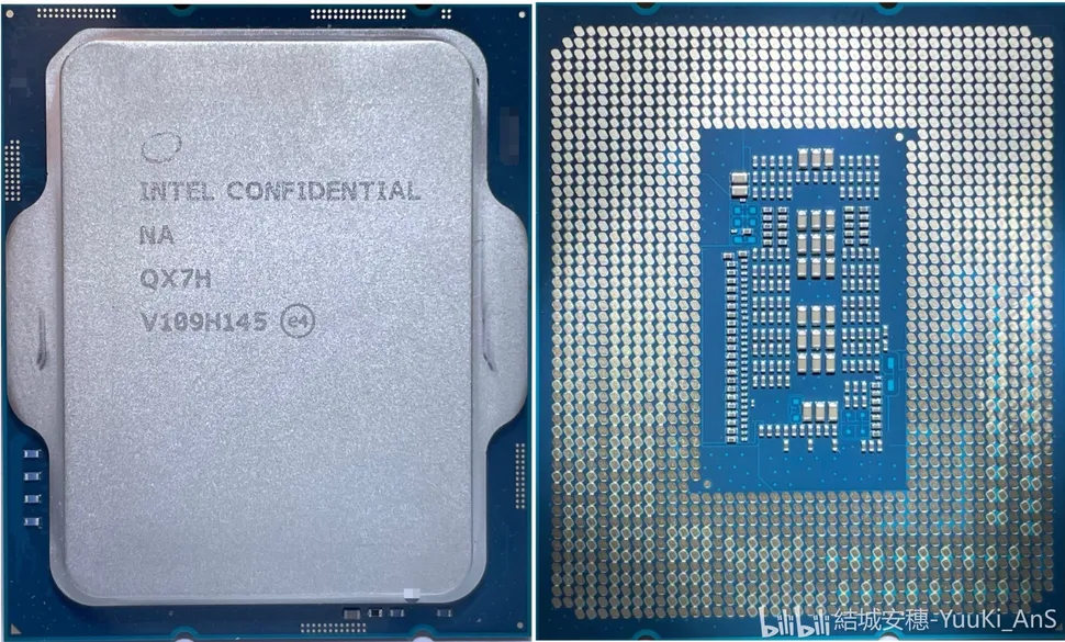
Last year, an Intel document revealed an LGA1700 interposer for its Alder Lake-S test platform, confirming that the rumored socket will likely house the new chips. Months later, an image surfaced at VideoCardz, showing an Alder Lake-S chip and the 37.5 x 45.0mm socket dimensions. That's noticeably larger than the current-gen LGA1200's 37.5 x 37.5mm.
Because the LGA1700 socket is bigger than the current sockets used in LGA1151/LGA1200 motherboards, existing coolers may be incompatible, but cooler conversion kits, which most cooler makers will provide for free for existing customers, can accommodate the larger socket. (Coolers that support both LGA11xx and LGA2066 already exist, so an in-between option isn't too difficult.)
The larger socket is needed to accommodate 500 more pins than the LGA1200 socket. Those pins are needed to support newer interfaces, like PCIe 5.0 and DDR5, among other purposes, like power delivery. Intel has also listed Alder Lake-S BGA support documentation, indicating that soldered-down models will also come to market.
PCIe 5.0 and DDR5 support give Intel a connectivity advantage over competing chips, but there are a lot of considerations involved with these big technology transitions. As we saw with the move from PCIe 3.0 to 4.0, a step up to a faster PCIe interface requires thicker motherboards (more layers) to accommodate wider lane spacing, more robust materials, and retimers due to stricter trace length requirements. All of these factors conspire to increase cost.

We recently spoke with Microchip, which develops PCIe 5.0 switches, and the company tells us that, as a general statement, we can expect those same PCIe 4.0 requirements to become more arduous for motherboards with a PCIe 5.0 interface, particularly because they will require retimers for even shorter lane lengths and even thicker motherboards. That means we could see yet another jump in motherboard pricing over what the industry already absorbed with the move to PCIe 4.0. Additionally, PCIe 5.0 also consumes more power, which will present challenges in mobile form factors.
Intel has announced that Alder Lake will support DDR5 memory, but that will cause pricing pressure. Notably, every transition to a newer memory interface has resulted in higher up-front DIMM pricing, which is concerning in the price-sensitive desktop PC market. DDR4 for example first came to the HEDT segment on Intel's X99 platform in 2014, and pricing at the time was more than double the cost of DDR3. Skylake brought DDR4 to the mainstream segment in 2015, but it still carried a 25-50% price premium.
DDR5 is in the opening stages; some vendors, like Adata, TeamGroup, and Micron, have already begun shipping modules. The inaugural modules are expected to run in the DDR5-4800 to DDR5-6400 range. The JEDEC spec tops out at DDR5-8400, but as with DDR4, it will take some time before we see those peak speeds.
We have, however, seen signs that only the higher-end Alder Lake desktop PC platforms, like Z-series motherboard, will support DDR5, while lower-end B- and H-series boards will use DDR4 for a friendlier price of entry. There have also been concrete reports that Intel will continue to use its new Gear 1 and Gear 2 memory alignment with Alder Lake. You can read more about this memory alignment, and the pros and cons, here.


It's no secret Intel has been struggling badly with TDP on its most recent desktop processors. The i9-9900K was the last 'sensible' chip at the top of Intel's product stack, with the i9-10900K capable of using 250W. We expect the same 250W max power use from Rocket Lake's i9-11900K. But Alder Lake should greatly improve the situation — though it's difficult to imagine how it could possibly be worse.
Traditionally, Intel has targeted a top TDP of around 95W for its mainstream CPUs, and we'd like to see a return of that approach. With the Enhanced SuperFIN 10nm process, Golden Cove high-performance cores, and Gracemont efficiency-focused cores, plus a larger IHS (integrated heatspreader) due to the larger socket, we expect Alder Lake to be far more competitive in TDP.
Additionally, the new desktop PC motherboards for Alder Lake chips will herald the arrival of mainstream ATX12VO motherboards that leverage a new lower-power PSU specification. Both systems with support for standard power supplies and the ATX12VO spec are planned, but Intel is on a full-court press to push the adoption of the new standard.
Intel 12th-Gen Alder Lake Xe LP Integrated Graphics
A series of Geekbench test submissions have given us a rough outline of the graphics accommodations for a few of the Alder Lake chips. Recent Linux patches indicate the chips feature the same Gen12 Xe LP architecture as Tiger Lake, though there is a distinct possibility of a change to the sub-architecture (12.1, 12.2, etc.). Also, there are listings for a GT0.5 configuration in Intel's media driver, but that is a new paradigm in Intel's naming convention so we aren't sure of the details yet.
The Alder Lake-S processors come armed with the 32 EUs (256 shaders) in a GT1 configuration, and the iGPU on early samples runs at 1.5 GHz. We've also seen Alder Lake-P benchmarks with the GT2 configuration, with 96 EUs (768 shaders). The early Xe LP iGPU silicon on the -P model runs at 1.15GHz, but as with all engineering samples, that could change with shipping models.
Alder Lake's integrated GPUs support up to five display outputs (eDP, dual HDMI, and Dual DP++), and support the same encoding/decoding features as both Rocket Lake and Tiger Lake, including AV1 8-bit and 10-bit decode, 12-bit VP9, and 12-bit HEVC.
Intel Alder Lake CPU Architecture
Intel pioneered the x86 hybrid architecture with its Lakefield chips, with those inaugural models coming with one Sunny Cove core paired with four Atom Tremont cores.
Compared to Lakefield, both the high- and low-performance Alder Lake-S cores take a step forward to newer microarchitectures. Alder Lake-S actually jumps forward two 'Cove' generations compared to the 'big' Sunny Cove cores found in Lakefield. The big Golden Cove cores come with increased single-threaded performance, AI performance, Network and 5G performance, and improved security features compared to the Willow Cove cores that debuted with Tiger Lake.
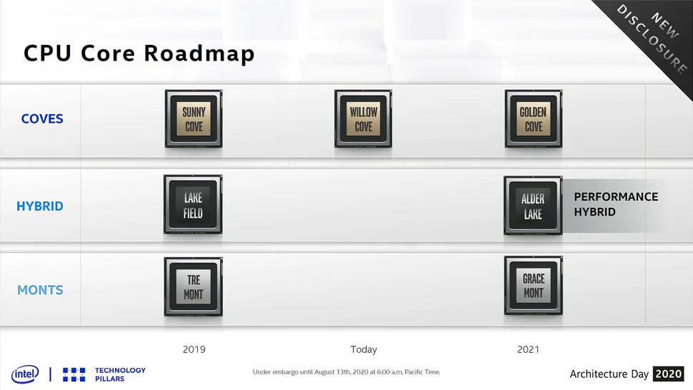

Alder Lake's smaller Gracemont cores jump forward a single Atom generation and offer the benefit of being more power and area efficient (perf/mm^2) than the larger Golden Cove cores. Gracemont also comes with increased vector performance, a nod to an obvious addition of some level of AVX support (likely AVX2). Intel also lists improved single-threaded performance for the Gracemont cores.


You can read our deep-dive coverage of the Golden Cove Performance Core architecture here. In summary, the Golden Cove microarchitecture is designed for low-latency single-threaded performance and comes with an average of 19% more IPC than the Cypress Cove architecture in Rocket Lake. It also supports AVX-512 and AMX (a new AI-focused matrix-multiply ISA) for data center variants (both are disabled on consumer chips).


You can also read our deep dive coverage of the Gracemont Efficiency Core architecture here. In summary, the single-threaded Efficiency (E) core, which comes with the Gracemont microarchitecture, is designed to improve multi-threaded performance and provide exceptional area efficiency (small footprint) and performance-per-watt. Four of these small cores fit in the same area as a Skylake core and deliver 80% more performance in threaded work (at the same power). A single E core also delivers 40% more performance than a single-threaded Skylake core (at the same power) in single-threaded work (caveats apply to both).


Lakefield served as a proving ground not only for Intel's 3D Foveros packaging tech but also for the software and operating system ecosystem. At its Architecture Day 2020, Intel outlined the performance gains above for the Lakefield chips to highlight the promise of hybrid designs. Still, the results come with an important caveat: These types of performance improvements are only available through both hardware and operating system optimizations. Let's look at Intel's solution to that problem.
Intel Thread Director
Intel unveiled the answer to the software challenge at its Architecture Day 2021 — the new Thread Director. Due to Alder's use of both faster and slower cores that are optimized for different voltage/frequency profiles, unlocking the maximum performance and efficiency requires the operating system and applications to have an awareness of the chip topology to ensure workloads (threads) land in the correct core based on the type of application.

The current thread scheduling systems are based entirely on static rules (priority, foreground, background) and tend to be inefficient and create software programming overhead. That's where Intel's Thread Director technology comes in. This hardware-based technology provides enhanced telemetry data to Windows 11 to assure that threads are scheduled to either the P or E cores in an optimized and intelligent manner, but in a way that's transparent to software.
This technology works by feeding the Windows 11 operating system with low-level telemetry data collected from within the processor itself, thus informing the scheduler about the state of the core, be it power, thermal or otherwise. (As we covered here, Intel has integrated a new power microcontroller in each Gracemont core, a first, that collects similar data on the order of microseconds instead of milliseconds, so it might be part of the new telemetry system.)

Additionally, Thread Director can also detect the instruction mix (scalar/vector) used in any given thread at a nanosecond granularity, and then communicate with the Windows 11 scheduler to steer the thread to the correct execution core, be that a high-performance P-Core or an efficient E-Core. Typically, vector/AI workloads will be prioritized to performance cores while scalar instructions and background tasks are moved to efficiency cores. However, the system is dynamic, so thread placement decisions can vary based on the dynamic mix of conditions and workloads present on the processor at any given time.
Additionally, threads can go through various phases and instruction mixes over their lifetime, so the scheduler constantly re-adjusts based on the real-time telemetry data. This is helpful when the number of threads designated for 'performance' outnumber the available cores, for instance. In that case, less demanding 'performance' threads, such as a program in a spin loop, can be moved off to the efficiency cores while more deserving workloads are assigned to the performance core.
Previously, the operating system didn't have access to this type of telemetry data to inform scheduling decisions, instead using simple data like whether the process was a foreground or background task. This enhanced system allows the operating system and processor to work in tandem to assure correct scheduling in real-time, thus avoiding costly software re-coding. This is a promising sign that existing code will run well on the Alder Lake processors.
Programmers can access more granular control, too, by specifying that certain threads are used in a certain manner through an expansion of the PowerThrottling API that allows developers to assign a QoS attribute to their threads. Additionally, a new EcoQos classification lets software tag threads that respond best on the efficiency cores to assure they are prioritized to execute on the E-Cores. Microsoft says that the Edge browser and 'various' Windows 11 components now take advantage of the EcoQos classification system, and we can expect support to broaden quickly.

This looks to be a promising and less-intrusive (at least from a coding standpoint) method of ensuring that the correct threads land on the correct cores, thus delivering optimal performance. That said, we'll have to see it in action before we can pass judgement on its efficacy – much of its potency will boil down to the latency involved with the process of communicating telemetry data and moving the thread, and intel isn't sharing those details yet. Additionally, it's possible that an excess of communication between the Thread Director and the Windows 11 scheduler could create a challenging workload of its own, so finding the right amount of granularity will be key to assuring both timely thread placement and a minimum of system overhead.
The system is already far in development, and Microsoft says that further enhancements to the engine are already underway and in planning for Windows 11, with more details to be shared at a later date.
Alder Lake chips will also work fine with a bog-standard Windows 10 operating system – existing thread-scheduling techniques continue to work with the processors, just not as well. While the chips work, you'll miss out on the enhanced capabilities of Thread Director (that's Windows 11 only), which will have a varying impact on performance and power consumption based on instruction type and application usage models. In other words, your mileage will vary.
The hybrid architecture could still result in some teething pains, as Intel itself recently divulged that some older games with DRM might not work with the new chips unless developers add specific software optimizations.
Finally, it has long been known that the Gracemont cores do not support the AVX-512 instruction set, and speculation has been rife about how the code would work on Alder Lake processors, if at all. Intel's answer is simple: AVX-512 will not work on either type of core present in Alder Lake. The high-performance cores do feature the Golden Cove architecture that supports AVX-512 natively, but Intel has fused that feature off (yes, the 512-bit FMA is still present and consumes die area) for the consumer chips. In contrast, server chips with Golden Cove have two 512-bit FMAs and fully support AVX-512. Meanwhile, the Gracemont cores are simply not AVX-512 capable, and disabling support allows the Alder Lake chip to have uniform ISA support.
Alder Lake comes to market in Fall 2021. We're sure to learn more at the inaugural Intel Innovation event October 27-28.
You may be interested in:
>> Is a Chromebook worth replacing a Windows laptop?
>> Find out in detail the outstanding features of Google Pixel 4a
>> Top 7 best earbuds you should not miss
Related Posts:
>> Recognizing 12 Basic Body Shapes To Choose Better Clothes
>>Ranking the 10 most used smart technology devices
>> Top 5+ Best E-readers: Compact & Convenient Pen

0 Comments:
Post a Comment